About the Project

Current Problem

There are currently no manufacturing technologies that can produce 3D metasurfaces on real products at commercially viable throughput. This is due to complex shape and size (<400nm) of the unit cell to be produced, which needs to be repeated in several layers.

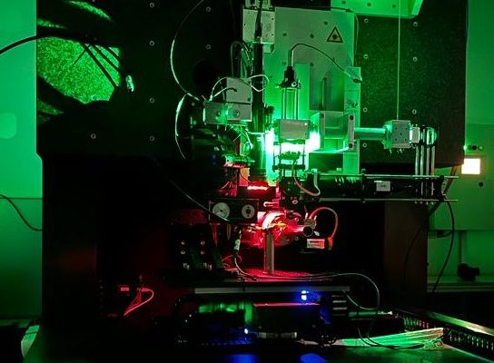
Classic 3D prototyping techniques (UV laser stereolithography, 3D inkjet printing), can produce 3D structures, but with resolutions limited to tens of micrometres; lithographic techniques with superior resolution (e-beam) are limited to producing planar 2D structures, and nanoimprint is both economic and high resolution, but hard to use in curved substrates. However, the current MPP process is inherently slow, as it involves a point-by-point translation of a focussed beam over a polymer sub-surface layer. Fabrication of a typical cm2 high-resolution component currently takes hours to even days. Making the process unsuitable for the industrial manufacture of multiple, complex features, in economically viable times.

What are metasurfaces and why are they important?

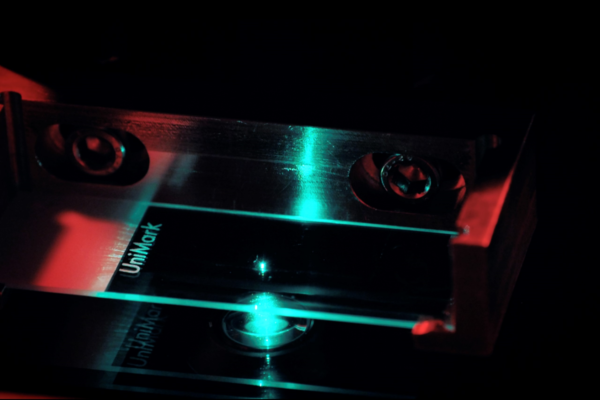
Optical metasurfaces are engineered thin films that manipulate the behaviour of light in a variety of ways. They consist of a two-dimensional array of subwavelength-sized structures that are carefully designed to interact with light in a precise manner.

The structures that make up an optical metasurface can be thought of as tiny antennas that can scatter, reflect, or refract light in a highly controlled way. By carefully designing the geometry and spacing of these structures, it is possible to create metasurfaces that can bend light in unusual ways, create complex optical patterns, or even generate holographic images.

Optical metasurfaces are important for several reasons. First, they offer a new way to manipulate light at the nanoscale, which is important for a variety of applications in fields such as photonics, sensing, and imaging. Second, they can be used to create flat, ultrathin optical components that are much thinner and lighter than traditional lenses or mirrors. This makes them attractive for use in compact, portable devices. Finally, because they are made using advanced nanofabrication techniques, optical metasurfaces can be tailored to specific wavelengths of light, making them ideal for use in a wide range of applications.

Our Solution

FABulous will overcome these difficulties by developing an industrial surface ‘coating’ technology that exploits breakthroughs in multiphoton lithography and process modelling to manufacture high resolution 3D metasurfaces at a throughput viable for series production.

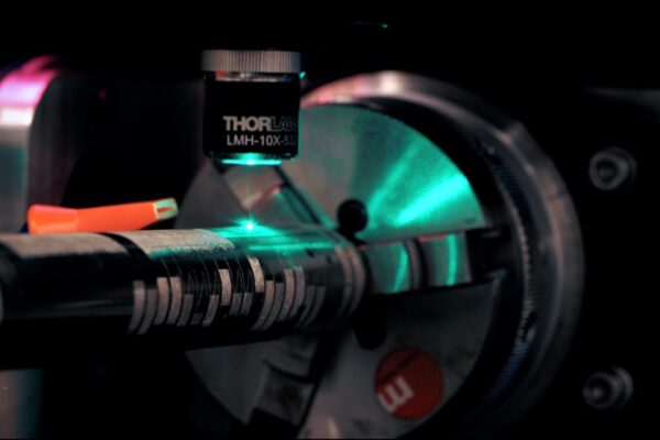
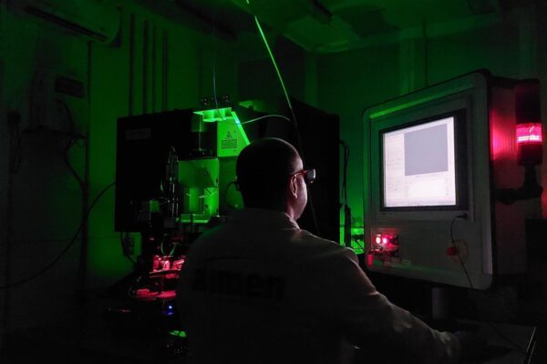
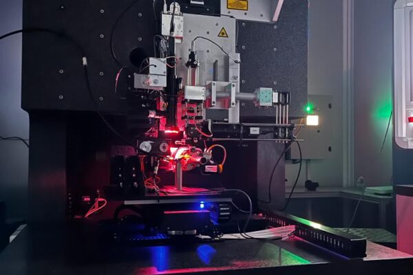
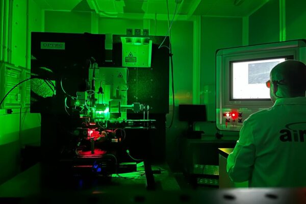
We will develop and demonstrate a new laser-based platform for the high-throughput and high efficiency manufacturing of optical metasurfaces. By co-optimising process, product, and surface design methodologies with new micro-fabrication methods, FABulous will enable the rapid fabrication of custom high-resolution 3D metasurfaces, at a throughput viable for commercial manufacturing. FABulous will also address the significant challenges that arise when applying the functional metasurfaces on irregular and curvilinear 3D substrates, polymer substrates or films. The fabrication of metasurfaces on products with complex geometries will be made possible through the development of AI driven digital models for real time integrated control of surface topology, focus, and beam wavefront correction.

These metasurfaces will be capable of manipulating light with unprecedented flexibility and will open the possibility of designing and manufacturing smaller, lighter, and more environmentally friendly products, through the replacement of bulky components and/or the chemical coatings currently used to enhance the efficiency and performance of optical products. These innovations will be scaled for commercial applications and integrated into an industrial platform (manufacturing of complex optical products including, sensors, automotive lights, and solar power generators) with a quality assurance and control system, enabling the fabrication of 3D metasurfaces on a range of substrates with unprecedented productivity, resolution, flexibility, and reliability.

Our Impact

The application of the technology and its potential to contribute to the design and manufacturing of more sustainable and circular European goods will also be demonstrated in a series of uses cases. The platform will be used to coat optical components (lenses, light pipes, and micro-optics arrays) with custom metasurfaces, and demonstrate that these components, when integrated into the design and manufacturing of functional optical systems (cameras, automotive lights and PV cells), can significantly improve their efficiency whilst in parallel reducing their environmental footprint.

Close Menu